- DME Channel on YouTube
Basically, a scanning probe microscope is an instrument for positioning a sharp tip at a defined distance above
the surface of some sample. In contradistinction to other positioning instruments, the scanning probe microscope
works on the nanometer scale. In standard modes, forces are measured in order to scan a surface topography, see
also the Introduction of Scanning Probe Microscopy.
Besides the mechanical interaction, however, a measuring tip can interact in many other ways with a surface.
Several different measuring methods exist, such as MFM (magnetisation),
SCM (capacitance), KFM (Potential), SSRM (resistance).
Here we want to present a variety of applications.
In order to get more information and images in higher resolution, click on the images.
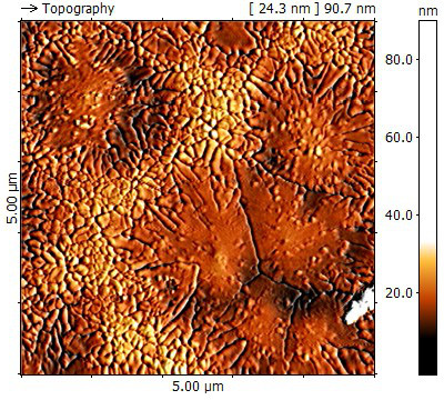
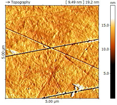
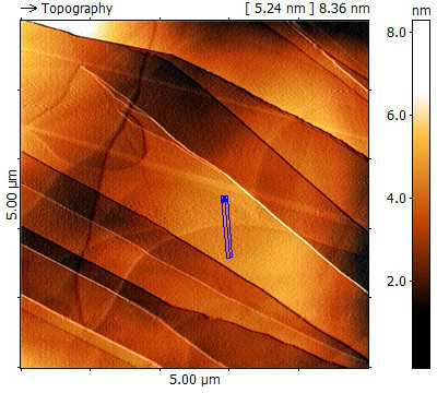
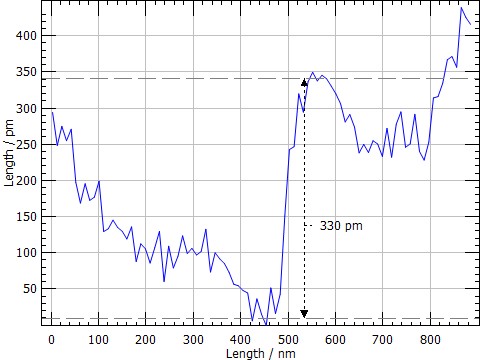
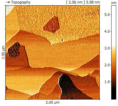
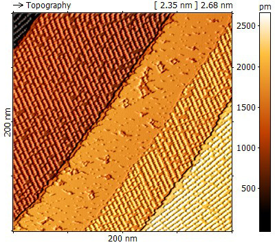
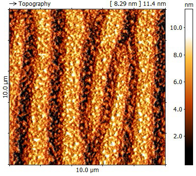
From left to right: PZT ceramics, surface of a polished glass lense, Atomic layer structure of HOPG (Highly Ordered Pyrolytic Graphite)
and height profile across one atomic layer (right)
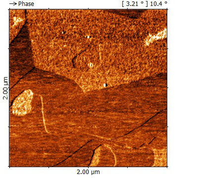
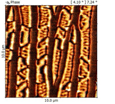
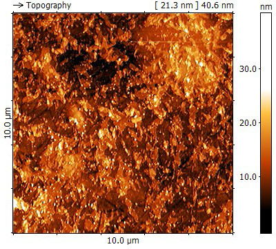
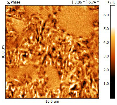
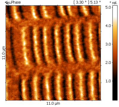
SiC and Graphene atomic layers: topography (left) and phase (right) are measured simultaneously.
From left to right:
Single atomic resolved UHV-STM image. Physik, Uni Marburg
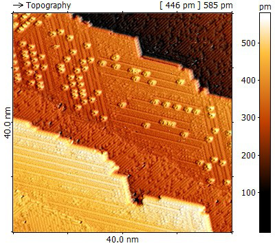
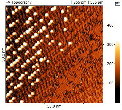
Nanodots on carbonized tungsten, UHV-STM. Physikalische Chemie, Uni Innsbruck
Nanodots on carbonized tungsten, UHV-STM. Physikalische Chemie, Uni Innsbruck
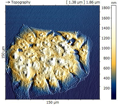
Colon cancer cells
Detailed information: The world seen by DME instruments - Topography
Magnetic samples: topography (links) and magnetic information, MFM, (right) are measured simultaneously.
Special steel: topography (links) and magnetic information, MFM, (right) are measured simultaneously.
Left: Nano structurized magnetic layer, DS95-50, color: magnetic information, shadow effect: topography.
PTB Braunschweig
Middle: Magnetic nano particles of different magnetisation are measured simultaneously.
Right: Magnetic information on a harddrive
Detailed information: The world seen by DME instruments - Magnetic sample
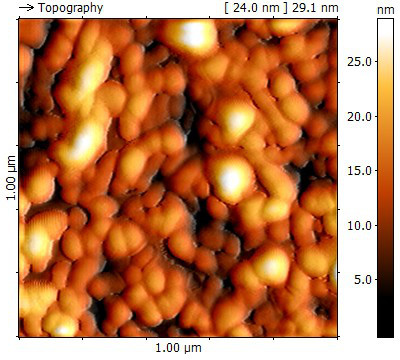
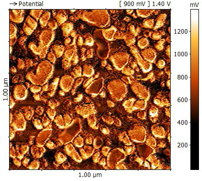
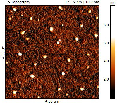
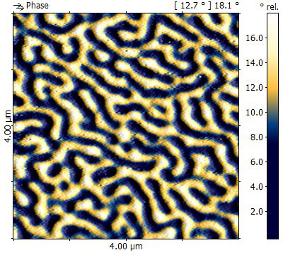
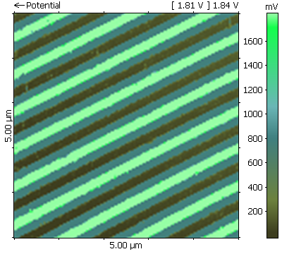
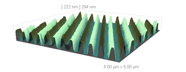
Nano particles on silicon: topography (left) and work function, KFPM, (right) are measured simultaneously.
Multilayer condensator: topography (left) and work function, KFPM, (middle) are measured simultaneously.
Detailed information: The world seen by DME instruments - Electrical properties

Photoluminescense measurements of optical semiconductors, Institut für Angewandte Physik,
Technische Universität Braunschweig
Detailed information: The world seen by DME instruments - Scanning nearfield optical microscope
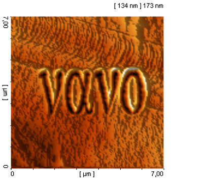
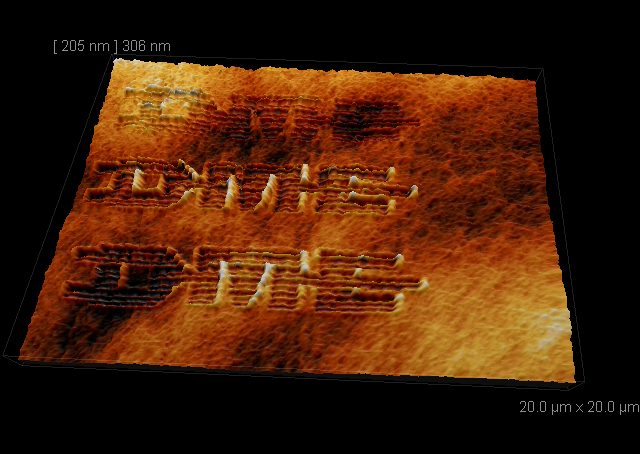
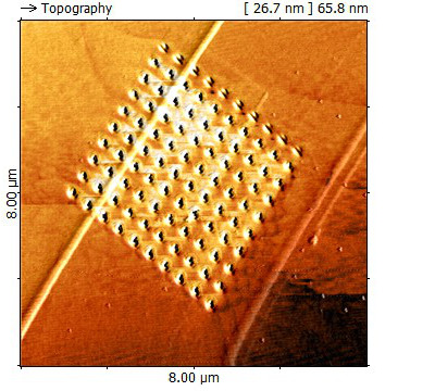
With a scanning probe microscope you can not only record information, but you can also
transfer information onto a sample.
Detailed information: The world seen by DME instruments - Lithography