- DME Channel on YouTube
Measured by: Institut für Angewandte Physik,
Technische Universität Braunschweig
Measured with: DS 45-40
One of the most versatile and at the same time also very complex SPM measurement technique is the optical nearfield microscopy (Scanning Nearfield Optical Microscope, SNOM or NSOM). This class of instruments are used for investigation of electromagnetic interactions (light) with a resolution below the wavelength of the used electromagnetic field. Also here are a lot of possibilities: With an apertureless SNOM you use a normal metal or semiconductor tip and use the electromagnetic interaction between the sample surface and the tip to amplify optical signals. If you illuminate the sample surface at the position of the tip, the interaction between the sample and light causes a light amplification and it is possible to obtain electromagnetic information in the order of magnitude of the tip geometry. This is used especially for amplification of Raman signals (Tip Enhanced Raman or Tip Enhanced Raman Spectroscopy: TERS).
Another possibility is to use a fine fiber glass tip to concentrate the light. This way, the fiber glass can be used for lighting as well as for collection of the detected light (Illumination Collection Mode SNOM), and it is possible to carry out photoluminescense experiments with resolutions below the light wavelength. This is especially interesting when a combination of CCD camera and monochromator is used as detector and measures a complete optical spectrum in each point of the surface (Optical Nearfield Spectroscopy). For a lot of investigations, this will be even more interesting, when these measurements can be carried out at very low temperatures. E.g. in optical semiconductors, many quantum mechanical effects can only be seen at very low temperatures.
With an optical nearfield spectroscope it is possible to make interesting animations by varying the detection wavelength. This page shows a number of photoluminescence measurements on optical semiconductors.
Each animation was made from the data of one single measurement.
Photo luminescence intensity dependent on wavelength
| Image data | |
| Image size: | 5 x 5 μm |
| Temperature: | ca. 50 K |
| Number of points: | 128 x 128 in x,y; 1024 in Z (Wavelength) |
| Total data size: | 33,5 MB |
| Spatially integrated opt. spectrum: | 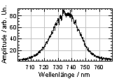 |
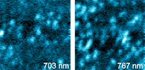
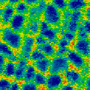
The video shows the wavelength dependent emission of InP (Indiumphosphid) quantum dots (embedded in GaInP, substrate GaAs). The sample comes from 4. Physikalischen Institut of Universtität Stuttgart.
At the edge of the emission spectrum only a few quantum dots are emitting, which looks like a random flashing at different locations. When the wavelength comes close to the emission maximum, more and more quantum dots start to emit. At the emission maximum, it is no longer possible to separate the individual emitting quantum dots, as their density is too large and the resolution capability is no longer sufficient. When the emission maximum is left, the density is reduced, so that at the other edge it is again possible to identify individual quantum dots.
If you look very closely, it is possible to see that at the long wave end of the emission spectrum the emission is seen as oblong forms, in contrast to the short wave end of the spectrum, where the forms are small and round. The oblong emission forms originate from coupled quantum dots. Is is very seldom possible to observe such effects directly.
- Coupling of quantum dots
Photo luminescence intensity dependent on wavelength
| Image data | |
| Image size: | 15 x 15 μm |
| Temperature: | Room temperature |
| Number of points: | 128 x 128 in x,y; 1024 in Z (Wavelength) |
| Total data size: | 33,5 MB |
| Spatially integrated opt. spectrum: | 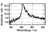 |
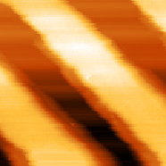
When a semiconductor structure is scratched, the grid constants are relaxed along the scratch. This leads to a change of the emission wavelength. This effect can easily be observed with the nearfield spectroscope. In the video you can clearly observe the "change" between the layer close to a scratch and the layers further away.
- Topography
Height difference
app. 350 nm
- Displacement of the maximum
Variation app. 4 nm
All information is measured simultaneously.
Photo luminescence intensity dependent on wavelength
| Image data | |
| Image size: | 15 x 15 μm |
| Temperature: | Room temperature |
| Number of points: | 128 x 128 in x,y; 1024 in Z (Wavelength) |
| Total data size: | 33,5 MB |
| Spatially integrated opt. spectrum: |  |
Emission of a normal blue InGaN LED at room temperature. The emission looks more like a cloud of points than a homogeneous emission. An InGaN LED structure grown on a sapphire substrate has many defects. Around the defects, no luminescence is present, thus the non homogeneous emission.
Photo luminescence intensity dependent on wavelength
| Image data | |
| Image size: | 20 x 20 μm |
| Temperature: | Room temperature |
| Number of points: | 128 x 128 in x,y; 1024 in Z (Wavelength) |
| Total data size: | 33,5 MB |
| Spatially integrated opt. spectrum: | 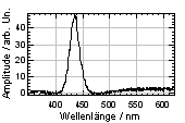 |
Often more things happen under the surface than the topography reveals. In this case the video shows dramatic differences of the luminescence, despite the fact that the topography in the dark areas looks similar to other areas.
- Topography
Height difference app. 400 nm
Photo luminescence intensity dependent on wavelength
| Image data | |
| Image size: | 10 x 10 μm |
| Temperature: | ca. 50 K |
| Number of points: | 128 x 128 in x,y; 1024 in Z (Wavelength) |
| Total data size: | 33,5 MB |
| Spatially integrated opt. spectrum: | 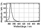 |
The sample consists of laterally grown layers with low defect density and vertically grown layers with higher defect density. The defects work as non radiative recombination centers, resulting in a strongly reduced luminescence around these. In the SNOM measurement it can be seen that the laterally grown layers are significantly brighter than the vertically grown layers.
Comparison with the (simultaneously recorded) topography image to the right shows that groves in the topography lie exactly in the middle of the laterally grown zones. (see F. Hitzel et al., Appl. Phys. Lett. 82, 4071 (2003) )
In the video it is clearly seen how the structure information is only visible for wavelengths within the emission peak. There are no reflections or similar effects that may cause a signal independent of the wavelength. It is one of the features of nearfield spectroscopy that through the wavelength sensitivity it is possible to distinguish between noise signals and real information.
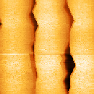
- Topography
Height difference app. 300 nm
-
- Peak width
Variation app. 2 nm
- Displacement of the maximum
Variation app. 1 nm
All information is measured simultaneously.
Photo luminescence intensity dependent on wavelength
| Image data | |
| Image size: | 10 x 10 μm |
| Temperature: | ca. 50 K |
| Number of points: | 128 x 128 in x,y; 1024 in Z (Wavelength) |
| Total data size: | 33,5 MB |
| Spatially integrated opt. spectrum: | 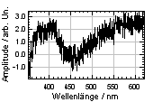 |
When growing, Indium-Gallium-Nitride is very sensitive to differences in the topography of the surface. By growing different layers on structured surfaces, it is possible with a SNOM to observe a number of different emission wavelengths.
In the spatially integrated optical spectrum, you can observe an increase of the intensity with longer wavelengths. This is an artifact by generated luminescence in the optics and in the beamsplitter. Since this disturbance is independent of the position on the surface, it is not visible in the optical images.
- Topography
Height difference app. 500 nm
Photo luminescence intensity dependent on wavelength
| Image data | |
| Image size: | 15 x 15 μm |
| Temperature: | ca. 50 K |
| Number of points: | 128 x 128 in x,y; 1024 in Z (Wavelength) |
| Total data size: | 33,5 MB |
| Spatially integrated opt. spectrum: | 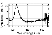 |
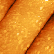
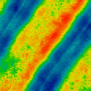
The topography shows that different crystal facets have been developed in the surface of this sample. On this structure were grown InGaN quantum films. If you look at the emission wavelengths of the different areas in the video, it is clearly seen that the tilted crystal facets shows a strongly blue displaced emission (more than 150 meV). This is a hint towards the defect inactivation mechanism in InGaN-LEDs, where tilted facets cause a high energy barrier around each defect. (see A. Hangleiter et al., Phys. Rev. Lett. 95, p. 127402 (2005))
- Topography
Height difference app. 750 nm
Photo luminescence intensity dependent on wavelength
| Image data | |
| Image size: | 7 x 7 μm |
| Temperature: | ca. 50 K |
| Number of points: | 256 x 256 in x,y; 1024 in Z (Wavelength) |
| Total data size: | 134 MB |
| Spatially integrated opt. spectrum: | 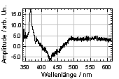 |
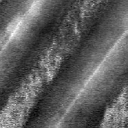
A high resolution scan with 256 x 256 points of a structure with a single InGaN quantum film at app. 50K. This is a partial laterally growing structure. Below the strong emission at the tilted crystal facets, you can still see the GaN emission at app. 360 nm. Please note the emission at app. 480 nm, which seem to run parallel to dislocations inside the material.

- Topography
Height difference app. 1400 nm