- DME Channel on YouTube
The principle of AFM relies on the interaction force between the AFM tip and the surface if both are brought in close proximity. The influence of this force on the cantilever is measured by a laser detection system and used to track the surface. To measure a surface profile, the cantilever is moved parallel to the surface (termed as x-y-direction). Thereby it encounters topographical features on the sample. This leads to a change of the interaction force between tip and sample. The system simultaneously readjusts the distance between tip and sample in the vertical direction (z-direction) using a feedback loop, in which the measured sensor signal is compared with a given sensor setpoint. The difference between these two values is the so called error signal. The error is adjusted to be zero by changing the distance between tip and sample. This z-correction as well as the error signal are recorded and resemble two kinds of surface profile. The z-correction directly gives the topography, while the error signal represents the gradient of the topography.
For measuring a rectangular area, this area is divided into multiple scan lines. These lines are combined to reproduce a three dimensional surface topography. The operation principle enables the AFM to detect atomic steps on the surface while, the lateral resolution is directly related to the cantilever-tip radius.
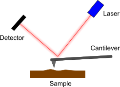
The most basic AFM operation mode is the so-called DC or contact mode. A force is applied to the cantilever (sensing)
tip when cantilever and sample surface are in close proximity. This leads to a bending of the cantilever, which changes
the reflectance angle of the detection laser. The deflection of the laser is measured by a position sensitive photo detector.
When the cantilever is moved towards the sample during the approach, attractive forces are applied to the cantilever.
These negative forces can be used to perform a surface scan.
There are two variations of the DC mode: In the constant height mode the cantilever is kept in a constant height to the
surface by regulating the force applied to the cantilever. The force variations then gives the image of the topography of
the sample. Whereas in the constant force mode, the deflection of the cantilever is hold constant by variing the distance
to the surface, which directly provides the topography of the sample.
Additionally to these mode variation, the lateral torsion of the cantilever can be measured and transformed to topography information.
Possible application: Topography measurements
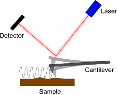
In order to prevent the cantilever from damages, most AFM microscopes are now usually operated in the so-called
AC mode instead of DC mode. In this mode, a very low force is used during scanning and very little interaction
between the surface and the cantilever occurs, without loosing resolution.
The cantilever is permanently vibrated with its resonance frequency. This oscillation leads to a periodic bending of
the cantilever which is measured by a reflected laser beam like in DC mode. When the cantilever is close to the surface
and interacts with surface atoms, the resonance frequency changes. (Actually the resonance frequency increases when the
cantilever reaches the surface.) This leads to a dampening of the amplitude and a phase change of the cantilever oscillation.
The tip-sample interaction force and the dampening of the cantilever oscillation are approximately proportional when the
tip is close to the sample.
The dampening of the amplitude as well as the phase change of the cantilever oscillation provides an image of the topography. In our ScanTool, usually the dampening is used for the topography, but the phase shift can also be recorded in an additional image.
The height interval of the proportional
relationship, from the point of increasing force to fully damped oscillation, depends on the oscillation amplitude and the
Q or qualitiy factor of the tip oscillation. The Q factor describes the relation between height and width of
the resonance peaks. The scanner sensitivity is enhanced with a higher Q factor of the actual resonance frequency.
Every cantilever has more than one resonance frequency, since it may oscillate in different directions and in different
ways. You must now find the frequency at which the cantilever tip oscillates most strongly. A good rule for choosing the
right resonance frequency is thus to select the peak with the highest Q factor in the area of the lowest occurring resonances.
AC mode works with less interaction force than DC mode and has some advantages:
- The surface itself is much less influenced by the measurement because of the low interaction forces.
- Because of the lower forces a single cantilever can normally be used for a larger number of images.
- Fragile samples which would be destroyed in a DC measurement can be imaged in AC mode.
- The relation phase shift / damping is characteristic for the surface material, therefore more information can be gained from this operation mode.
Cantilevers required for each mode of operation differ from each other: The DC mode cantilevers are longer and thinner than AC mode cantilevers, in order to get a strong cantilever bending at small forces. To minimize oscillation amplitude and increase the Q factor, AC mode cantilevers are shorter and thicker.
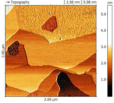
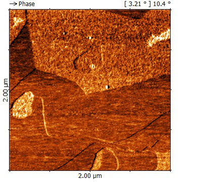
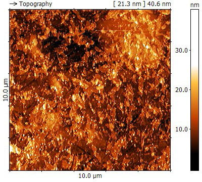
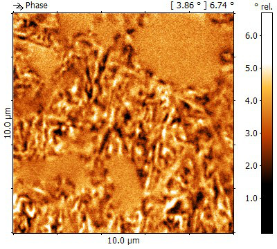
SiC and Graphene atomic layers: topography (left) and phase (right) are measured simultaneously.
Possible application: Topography measurements
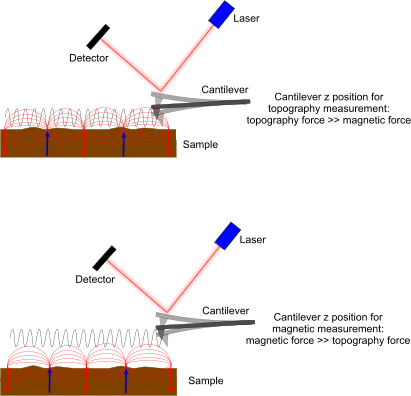
To be able to detect magnetic forces, one has to use a cantilever which is coated with a magnetic coating. Standard MFM tips have a magnetic coating with a relatively large thickness of around 40 nm. The high thickness results in a much larger tip radius of around 50 nm, which is much larger than that of conventional AFM tips. With these standard tips one can obtain lateral magnetic resolutions of about 100 nm. So, the magnetic resolution is much less than the resolution one can commonly expect from AFM topography measurements, which are a factor of 10 better. One will get already the maximum MFM resolution when scanning a 10 x 10 µm area with 128 x 128 pixels.
When the MFM tip is close to the sample, mechanical force as well as magnetic force contribute to the
force that is measured by the cantilever. The magnetic force is much smaller then the mechanical force but
is effective over a long distance. To separate the two force sources, the MFM force must be measured at a certain distance
to the sample surface, where the contribution from the mechanical force can be neglected.
This leads to the following measurement principle:
- For each scan line of the AFM image first the topography is measured.
- The tip is moved away from the surface by a certain distance. Then the same line is scanned again and the tip is moved parallel at a constant distance to the surface, using the information from the topography measurement before.
The magnetic force can now be measured in three different ways:
- Cantilever Bending:
- The magnetic force causes a bending of the cantilever, depending on the magnetig field strength. As the magnetic forces are low, one has to use a cantilever with low force constant. Commonly this type of measurement is performed when the scanner is running in DC mode, because then there is no other possibility of measuring the magnetic force.
- When the scanner is running in AC mode, then this bending is overlaying the tip oscillation. To eliminate the oscillating part, the signal has to go through a low pass filter.
- Measuring magnetic forces by cantilever bending is the method with the lowest sensitivity.
- Oscillation Amplitude Damping:
- When the scanner runs in AC mode, the magnetic field causes a damping of the cantilever oscillation. So the oscillation amplitude is also a measurement of the magnetic force.
- This method has medium sensitivity.
- Oscillation Phase Change:
- When the scanner runs in AC mode, the magnetic field causes a phase shift in the cantilever oscillation. The phase of the oscillation is much more sensitive to external forces than the oscillation amplitude because the phase shift occurs at much lower forces than required to measure a damping of the oscillation. Measuring the oscillation phase is the method of choice for obtaining high quality MFM measurements.
There are different magnetic probes available on the market. One difference is the magnetic field strength at the tip. A strongly magnetized tip can easily change the magnetization of a magnetically weak sample. At the same time, a cantilever with a strong magnetization is more sensitive to the magnetic field from the sample. So the cantilever must be chosen as a compromise between image quality and maximum magnetic field strength.
Special steel: topography (links) and magnetic information, MFM, (right) are measured simultaneously.
Possible application: Measurements of magnetic samples
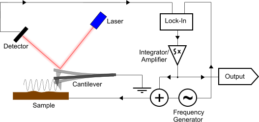
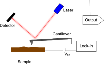
This mode is a method to determine the chemical potential between a cantilever and a sample surface, and therefore get information about the material and material state on a sample's surface. The basic setup for a KPFM measurement is shown in the figure beside. The sample is electrically connected to the output of a frequency generator. This creates an oscillating electrical field between cantilever and sample, which can be measured by the position sensor of the AFM. This detected signal is then fed into a lock-in amplifier and its output is put into an integrator. The result is then added as a constant offset to the oscillation which is applied to the sample. This acts as a feedback loop, which minimizes the electrically induced cantilever oscillation.
When applying a voltage between the cantilever and sample, an electrostatic force appears at the cantilever which can be in
be described by
F = -1/2 dC/dz V2
with V = VDC - VCPD + VAC * sin(ωt).
Hereby C is the capacitiy, VDC denotes the constant part of the applied voltage, VAC the oscillating part of the applied
voltage and VCPD a voltage created by aligning the two fermie levels of the cantilever and the sample surface
(contact potential difference voltage).
Inserting the voltages into the force equation yields a long term, which can be sorted with respect to the frequencies
to F = FDC + Fω + F2ω.
With the further assumption, that the capacity C is propotional to 1/d the terms of F can be written as:
FDC ∝ C * (VDC-VCPD)2 + VAC2 /2,
Fω ∝ C * (VDC-VCPD) * VAC * sin(ωt),
F2ω ∝ C * VAC2 * cos(ωt).
In the KPFM Fω is used: When VDC equals VCPD this force disappears. So, the
output of the feedback loop corresponds to VCPD which is the chemical potential.
For capacity measurements, one can look at F2ω, which is directly proportional to the capacity C between
tip and sample surface.
For KPFM measurements, a conductive cantilever is needed. Commonly so-called EFM cantilevers are used. These are longer
than conventional AC cantilevers and provide a better signal to noise ratio because they react stronger on electrical field
changes. As standard cantilever are made of highly doped silicon, these can also be used for KPFM measurement. The creation
of a P/N junction on the sample surface by this less problematic than in current measurement mode, as the KFPM method only
uses AC voltages. When taking a standard cantilever, care should be taken that the cantilever body is electrically connected
to the AFM's cantilever holder.
One of the critical points in a KPFM measurement is choosing the right frequency. The frequency should be at least be
10 to 20 kHz away from the current working frequency of the AFM scanner, otherwise interference will occur between the
normal AC mode oscillation and the electrically induced oscillation.
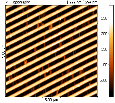
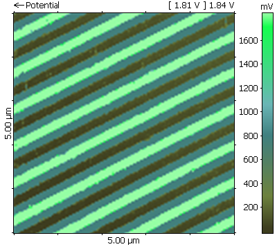
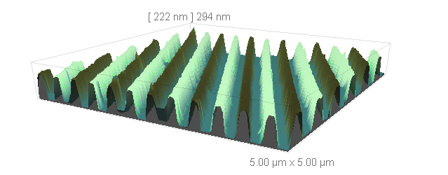
Multilayer condensator: topography (left) and work function (middle) are measured simultaneously.
Superposition of both images: 3D structure = topography, color = work funktion
Possible application: Electrical properties
This method is used to determine the relative changes of majority carrier concentration of flat semiconductor surfaces. The capacity measurement is done quite similar to the KPFM measurement. You can use the same measurement setup. The main differences are that the output is coming from the lock-in amplifier, not from the feedback signal, so one uses the force component F2ω, described above at KPFM, which is proportional to the capacity C between tip and sample surface.
The capacity measurement also results in relative information about the capacity. The absolute capacity between tip and a conducting sample is in the range of aF (atto farad = 10^-18 farad) where the capacity between cantilever body and sample is in the range of fF (femto farad = 10^-15 farad). These small dimensions and the large offset show that a direct measurement of the capacity is nearly impossible and also there, only relative values can be obtained.
A KPFM measurement of the electrostatic force without a nulling feedback regulator is called EFM, electrostatic force measurement. Here, the feedback regulator is left out and the output of a lock-in amplifier is directly monitored. This measurement shows, as seen in the equation Fω derived above for KPFM, a mixture of different information and is influenced by the chemical potential, the oscillation voltages, the capacity etc. Therefore the EFM method is less useful for determining physical properties than the KFPM method.
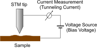
The STM mode has the most simple principle and works only with conducting samples. A metall tip perpendicular to
the sample surface is used instead of a cantilever. The tip as well as the sample are connected to a voltage supply.
Now the STM tip is brought so close to the sample that a current flows, a so-called tunnel current.
There is an exponential connection between the tip to sample distance and the current flow.
There are two variations for scanning: In the constant height mode, the height of the tip and the voltage is kept
constant, while the tunneling current changes. For an images, this changes are translated to topography information.
In the constant current or feedback mode, the tip is moved up and down to maintain a constant tunnel current, thereby
the tip is moving in a constant distance to the surface. The necessary up and down movements of the tip are electronically
recorded and can be displayed as an topography image.
Even though this principle is very simple, it instantly delivers the maximum possible magnification and allows the investigation and manipulation of individual atoms. The reason for this is a kind of self-focusing effect: The tunnel current responsible for the imaging already flows over the atom on the tip which is closest to the sample surface. So even when using a tip cut just by an ordinary pair of pincers one quite often gets atomic resolution.
The voltages used for STM measurements are normally below 1 V, since the electric field between sample and
tip created by the fine tip is very large. An applied voltage of 5 V already results in a strong electric
field causing a displacement of the tip and the sample surface. Actually, a 5 V pulse is often used
for "cleaning" the tip.
The tunnel currents are on the nA scale, and the distance between tip and sample are in the order of magnitude of
a few nm. STM measurements require that the sample surface is atomically "clean". In air, it is only
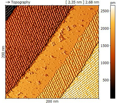
possible to obtain atomic resolution for certain samples. The easiest atomic grid to observe is that of an HOPG
sample (Highly Oriented Pyrolytic Graphite) since the top layer from such a sample can be removed by means
of a piece of adhesive tape, revealing for a short time an atomically "clean" surface. Therefore, such samples
are often used as test structures for STM microscopes; all DME STMs are tested for atomic resolution with a HOPG sample
as a part of our internal certificate of complience (CoC) test.
The STM scanning is very fast; for atomic resolution images you can usually achieve a scan rate of multiple images per second.
From left to right:
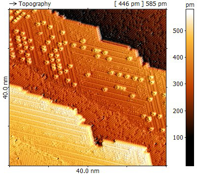
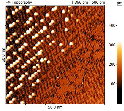
Single atomic resolved UHV-STM image. Physik, Uni Marburg
Nanodots on carbonized tungsten, UHV-STM. Physikalische Chemie, Uni Innsbruck
Nanodots on carbonized tungsten, UHV-STM. Physikalische Chemie, Uni Innsbruck
Possible application: Topography measurements
In this method also an conductive probe is used. Operating in DC mode, an DC bias is applied and the electric current between the tip and the sample is measured. The resulting resistance is caused by the spreading resistance and resistivity of the sample which also give information about the carrier distribution.
Note, that you have to scratch the surface of the sample with the tip to get a better electrical contact.
The typical radius of SPM sensors is in the order of 10 nm. So it is possible to perform lithography on a scale of only a few
nanometers.
Doing a lithography means that physical or chemical properties of a sample's surface are being changed. This can be done in three
different ways:
- exposing the sample with light or electrons,
- applying high pressures (scratching),
- applying electrical fields.
The main idea of the SPM program lithography function is to transfer the information of a bitmap via physical properties like a force, a voltage or a current to the surface. Depending in which mode (AFM-AC, AFM-DC, STM) the SPM is running, the physical property can be a bias or a current (STM), a force variation (AFM) or voltage at the auxiliary port of the controller (all modes). The Aux voltage can be converted into many other physical properties using external equipment.
Assume the surface of an AFM tip to about 100 nm2. If a tip with a force constant of 50 N/m is pressed 200 nm towards the surface, the resulting force equals about 10-5 N. The pressure applied to the surface is of about 100 GPa. This means that on almost any surface softer than the silicon tip, patterns may be scratched into the surface.
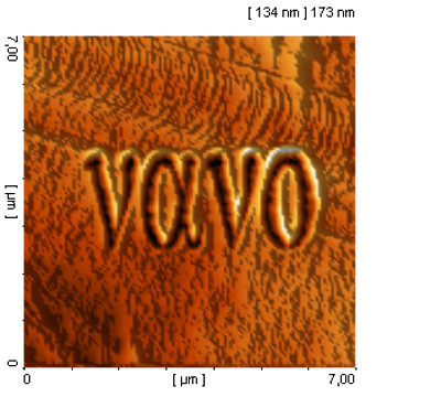
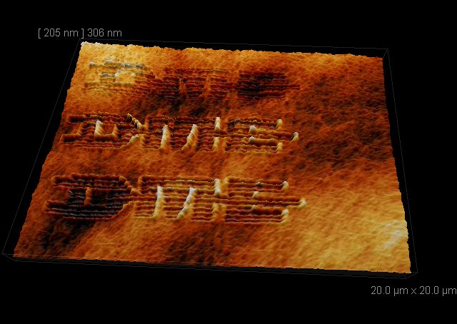
Possible application: Lithography