- DME Channel on YouTube
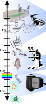
The maximum obtainable magnification with a conventional optical microscope is app. 800 to 1000 times, because of the nature of light. For further magnification Scanning Electron Microscopes (SEMs) are used, and among these the Transmission Electron Microscopes (TEMs) can show single atoms and thus provide the highest possible magnification. Why then do we have the Scanning Probe Microscope, SPM as yet another type of microscopes?
One of the reasons is that a sample to be examined in a transmission electron microscope must be sliced thinly and thus ruined. The SPM technique images surface structures with atomic (height) resolution without the necessity of damaging the sample. A further reason is the kind of imaging offered by SPM microscopes the results are shown as a kind of three-dimensional image (also in cases where only two-dimensional information is evaluated). As is the case with an optical microscope, it is very difficult to investigate the surface structure of a sample with an electron microscope. In order to measure a surface profile with the highest resolution, it is necessary to slice the sample. Moreover, an SPM operates without vacuum, and in contradistinction to electron and optical microscopes it can measure different other physical effects. This includes electrical properties such as e.g. Kelvin Probe Force Microscopy (KPM / KPFM) or magnetic properties (Magnetic Force Microscopy, MFM).
Basically, two main types of SPM microscopes exist: Scanning Tunneling Microscopes (STMs) and Atomic Force Microscopes (AFMs). In both cases an image is recorded by mechanically moving a fine tip as a sensor close to the surface in lines across the sample - the sample is scanned In this case, "fine tip" means a tip with a radius in the range 1 to 10 nm. Also in this case, "close to the surface" means in a distance of a few nm. During a scan the surface is normally "sensed" and from this information comes an image of the surface. For the scanning movement, either the sample or the tip can be moved; in the first case you speak of a Probe Scanner; in the latter of a Sample Scanner.
The way for sensing the surface differs between STMs and AFMs:
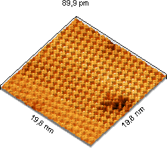
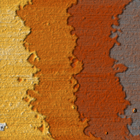
- STM measurement with atomic resolution
Sulphur on a Cu100 surface (Measurement performed at Technical University of Denmark)
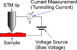
The STM has the most simple principle and works only with conducting samples. The metal tip as well as the sample are connected to a voltage supply. Now the STM tip is brought so close to the sample that a current flows, a so-called tunnel current. There is an exponential connection between the tip to sample distance and the current flow. During a scan, the tip is moved up and down to maintain a constant current, thereby the tip is moving in a constant distance to the surface (at least if the material is the same everywhere...) The necessary up and down movements of the tip are electronically recorded and can be displayed as an image. Alternatively, instead of moving the tip, in some microscopes the sample is moved up and down, which actually doesn't matter as long as the sample is fixed good enough to the sample holder. Even though this principle is very simple, it instantly delivers the maximum possible magnification and allows the investigation and manipulation of individual atoms. The reason for this is a kind of self-focusing effect: The tunnel current responsible for the imaging already flows over the atom on the tip which is closest to the sample surface. So even when using a tip cut just by an ordinary pair of pincers one quite often gets atomic resolution.
The voltages used for STM measurements are normally below 1 V, since the electric field between sample and tip created by the fine tip is very large. An applied voltage of 5 V already results in a strong electric field causing a displacement of the tip and the sample surface. Actually, a 5 V pulse is often used for "cleaning" the tip.
The tunnel currents are on the nA scale, and the distance between tip and sample are in the order of magnitude of
a few nm. STM measurements require that the sample surface is atomically "clean". In air, it is only
possible to obtain atomic resolution for certain samples. For measurements in air, undesired molecules or atoms
will often adhere to the surface and prevent a recording of the original structure. The easiest
atomic grid to observe is that of an HOPG sample (Highly Oriented Pyrolytic Graphite)
since the top layer from such a sample can be removed by means of a piece of adhesive tape, revealing for a short
time an atomically "clean" surface. Therefore, such samples are often used as test structures for STM
microscopes; all DME STMs are tested for atomic resolution with a HOPG sample as a part of our internal certificate
of complience (CoC) test. Nonetheless, even with such samples, and irrespective of the brand of STM used, it is more
of an art than science to achieve images with atomic resolution. Because a clean, atomic resolution image is only
obtained, when the tunnel current flows over just one atom from the STM tip instead of moving back and forth between
several atoms. However, once you get a good image, in most cases the following images will also be good.
The STM scanning is very fast; for atomic resolution images you can usually achieve a
scan rate of multiple images per second.
- Atomic steps of strontium titan oxide, step height 0.78 nm
Measurement made at Institut fü elektr. Messtechnik, TU Braunschweig
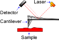
The AFM uses another detection principle. Here the sensor is a thin beam with a fine tip at the front end, called a cantilever. A laser beam is focused onto the upper side of the cantilever and reflected onto a position detector. This way it is possible to measure the bending of the cantilever. The length of the cantilever is a few hundred micron, while the thickness is only a few microns, so very little force is necessary to bend the cantilever. This force measurement can be used for a mechanical scanning of the sample surface.
In contradistinction to STM, AFM can also be used on non-conductive samples. AFM operates in different modes; the simplest one is the so-called contact mode or DC mode. Here it is attempted during a scan to keep constant the bending of the cantilever, i.e. the force with which the cantilever presses on the sample, and mechanically move the cantilever up and down correspondingly. The up and down movement is detected like in an STM, and you get an image of the surface. Here, the forces occurring between sample and cantilever are on the nanonewton scale. Often these forces are too large for the sample, and may also cause the cantilever tip to become worn or dirty.
For this reason, most AFM microscopes are now usually operated in another mode, the tapping mode or AC Mode. Here the cantilever is excited with its resonance frequency, so that it is permanently oscillating. Hereby, also the laser beam and the detector voltage are oscillating, and it is possible to measure an electrical signal proportional to the mechanical oscillation amplitude of the cantilever. When exciting with the resonance frequency, only a very little energy is necessary to maintain a strong oscillation. If the oscillating cantilever is brought close to the sample surface, the cantilever oscillation will be damped even at very small forces between sample and cantilever. The forces occurring between sample and cantilever are here one to two orders of magnitude smaller as for contact mode (app. 0.1 nN). This results in fewer influences on the sample surface and in a longer lifetime of the cantilever tip. At the same time, the influence on the resolution of this operation mode is negligible, for which reason it has become the most commonly used mode.
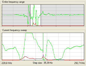
Before you can perform measurements with a cantilever in AC mode, its resonance frequency must be determined. For this, the frequency spectrum (i.e. the oscillation amplitude at different frequencies) is measured. The resonance frequency is seen in the frequency spectrum as a Peak with a certain width and height. Every cantilever has more than one resonance frequency, since it may oscillate in different directions and in different ways. You must now find the frequency at which the cantilever tip oscillates most strongly. Luckily, in most cases it is the lowest occurring resonance frequency. A further characteristic is the relation between height and width of the resonance peaks, called the Q factor. The scanner sensitivity us enhanced with a higher Q factor of the actual resonance frequency. The Q factor is a measure for the quality of an oscillating system and is related to the damping of the oscillations. For an oscillating cantilever, commonly the smallest damping occurs when the total tip is oscillating in its lowest mode. A good rule for choosing the right resonance frequency is thus to select the peak with the highest Q factor in the area of the lowest occurring resonances. Nowadays, the measurement of the frequency spectrum and the selection of the right peak is normally made automatically without interference from the user. In this respect, working in AC mode is not that different from working in DC mode. The diagrams above right show a screen shot from the DME SPM Windows(c) program of the frequency spectrum of a cantilever and the found peak. The red curve is the oscillation amplitude, whereas the green curve is the phase displacement.
Almost all Scanning Probe Microscopes are capable of resolving atomic height steps. AFMs can also reach a lateral atomic resolution. This puts severe requirements on the tip geometry, however, and is extremely difficult to achieve with normal cantilevers with a tip radius of 10 nm. Also in normal air atmosphere every surface has some adsorbed molecules hiding the real surface from the AFM tip. Only a few surfaces allow lateral atomic resolution in air. In this connection, the STM has the advantage that the tunnel current always flows directly over the next atom on the sample surface. This kind of "self focusing" does not occur with an AFM. AFMs with lateral atomic resolution are only used for special cases, where achieving a lateral atomic resolution is more important than the loss of flexibility, brought on by the higher stability of the total set-up. Normal AFMs are designed for relatively large scan areas (50 to 200 µm) and the scanner stages allow investigation of many different types and sizes of samples.
On the contrary, STMs are usually integrated into a highly stable scan platform, and the maximum scan area is around 0.5 to 10 µm. Moreover, the necessary stability of the scan stage only allows small sample sizes and heights. Often STMs are used in Ultra High Vacuum, so that a prepared sample surface may remain uninfluenced for a longer time.
Besides the topography, Scanning Probe Microscopes can also measure other physical parameters. As an example, simultaneously with an AFM scan, a current flow can be measured, or the phase displacement of the cantilever oscillation as well as several other physical properties. It is also possible to record spectrums, U/I curves, or other information in selected or all points on the surface, and it is possible to manipulate the surface. The Scanning Nearfield Optical Microscope (SNOM) is an example of an extended AFM in which additionally to the topography also electromagnetic information (light) is recorded. A look at data sheets from SPM manufacturers reveals a vast number of mostly three-letter abbreviations, showing the diversity of possible measuring methods. With an electrically conducting, bendable tip which can be positioned with great accuracy, it is possible to measure yet a vast number of physical parameters.