- DME Channel on YouTube
Nearly all semiconductor devices are made of hetero structures, stacked layers of different materials deposited with different techniques. Thicknesses of these layers are in the range of micrometers down to nearly single atomic thickness. For the correct operation of an electronic device, the electronic configuration at layer interfaces is essential. Even though the electronic properties of such interfaces can be simulated, many physical effects caused by the deposition process and layer interactions influence the interface in a certain and often non predictable way.
Here, we present a powerful way of performing an in-situ analysis of hetero structure interfaces using an organic solar cell structure as an example. The method and the work presented here were developed and performed by Saive et al. [1]. Interfaces have been electrically characterized by Scanning Kelvin Probe Force Microscopy (SKPM). Like in a conventional kelvin probing system, the SKPM method provides information about the work function (chemical potential) difference between a sensing tip and the sample surface. For SKPM, an atomic force microscope (AFM) tip is used as a kelvin probe sensor, which allows to measure work function variations with extremely high lateral resolution, in some cases down to the atomic level. The work function is determined by the intrinsic potential of a material, the electronic configuration like carrier density and type, and an eventually applied electrical potential. Performing a SKPM measurement on a cross section of a hetero structure, results in absolute measurements of work function differences between the different layers. This also enables the direct measurement of the voltage drop between the different layers if an external voltage is applied across the hetero structure.
The surface of an organic semiconductor is very sensitive to air exposure, so these semiconductors have to be encapsulated in air tight containers. To perform high resolution electrical characterization, exposed surfaces have to be protected from contamination by air. The combination of the Carl Zeiss AURIGA crossbeam work station and the Carl Zeiss AFM option for MERLIN allows preparation and investigation of the solar cell without the need to expose the prepared structure to air.
The investigated solar cell was a bulk hetero junction solar cell (BHJ) with P3HT:PCBM used as active layer. The solar cell was fabricated on an indium tin oxide (ITO) coated glass by spin coating first a 25 nm thick PEDOT:PSS buffer layer and then about 200 nm P3HT:PCBM which we call the BHJ layer (see [1]). The top contact consisted of 0.6 nm LiF and a 100 nm Al top layer. In order to prepare defined contact structures, the substrate was patterned by a photolithographic process before spin coating the active layers.
As a first step, a trapezoidal trench was milled into the cell by the focused ion beam. This resulted in a cut through the sample under a 54° angle. The resulting cut is shown in Fig 1.
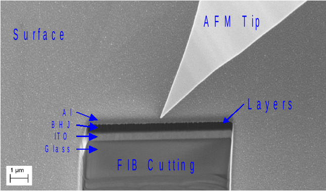
- Fig 1: Sample after preparation by FIB
After preparing the sample, the layer structure could be directly investigated by the AFM. The Carl Zeiss AFM option is designed in such a way, that the AFM tip is always in the vicinity of the crossbeam point, the intersection of SEM and FIB beam. Therefore, the target area can immediately after preparation be investigated by the AFM. All procedures to relocate the cut out area with an ex-situ system is avoided as the sample is already positioned at the right place.
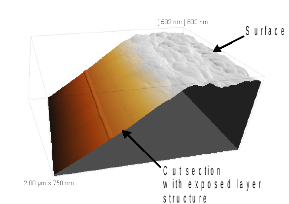
- Fig 2: AFM micrograph showing the 3D topography of the cut out section
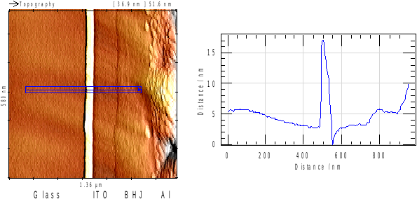
- Fig 3: Flat cut section only, the layer structure can also be seen in the topography due to different ion milling behavior of the different materials
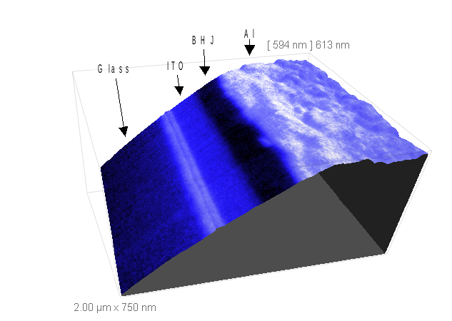
- Fig 4: Topography combined with work function signal
With the Carl Zeiss AFM option it is also possible to investigate a sample under operation: In the next experiment, the top and bottom of the solar cell structure have been electrically connected, so that is was possible to electrically ground the top or the bottom or both sides of the solar cell. Additionally, the solar cell had been mounted on a sample holder with a built-in LED (see Fig. 5), so that it was possible to control the illumination of the sample at the same time.
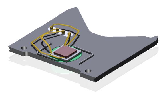
- Fig 5: The special sample holder for the AFM option has four user defined electrical feed throughs. The figure shows the sample holder with a led in the white spacer below the sample. Two of the electrical contacts where used to power the LED and the other two connect the top and bottom contact of the solar cell structure
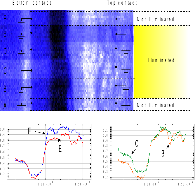
- Fig 6: SKPM image with different configuration of the solar cell and the resulting work function curves.
These experiments show, that the dominating open-circuit voltage drop occurs on the Al-BHJ interface. Without giving
further measurements here, it could also be shown, that when applying a voltage between bottom and top contact (instead
of grounding), the dominant voltage drop occurred still at the Al-BHJ interface.
In an optimal solar cell, the voltage drop should not occur at the interfaces but be distributed linear across the active
layer. In the present case this means that the Al-BHJ interface behaves sub optimal and has a high resistance. Even though
the sub optimal behavior of this cell could be measured by macroscopic measurements as well, only this investigation made it
possible to point out the Al-BHJ interface undoubtedly as the reason for the suboptimal behavior.
The combination of the Carl Zeiss AURIGA crossbeam workstation and the Carl Zeiss AFM option for MERLIN was used to identify a high interface resistance as the reason of inefficiency of a certain organic solar cell type. This investigation technique can be applied to basically all hetero structures, to test internal interface resistances and layer behaviors.
The method can also improve investigating materials, which are commonly air resistant like conventional inorganic semiconductor structures. As the scanning kelvin probe technique is very sensitive to the upper most atomic layers, air exposure of the investigated surface often leads to disturbances and a low signal to noise ratio. Furthermore, this method allows to directly target certain regions on the semiconductor e.g. on laterally structured semiconductors. It can also be used for defect investigation to get electrical information of structures buried below the surface.
- Rebecca Saive, Michael Scherer, Christian Mueller, Dominik Daume, Janusz Schinke, Michael Kroeger, Wolfgang Kowalsky,
Imaging the electric potential within organic solar cells, Advanced Functional Materials Volume 23, Issue 47, December 2013, Pages 5854-5860