- DME Channel on YouTube
The Carl Zeiss AFM option for FE SEM opens new possibilities in the analysis of beam based patterning methods. Since the Orion series is available, the dimension of generated patterns could be reduced to single digit nm values. The ability to generate this pattern carries the need to be able to analyze it with high resolution and 3D. Since 3D SEM is at it limits at this scale, this task can only be carried out by Atomic Force Microscopy (AFM). The AFM option from Zeiss combines SEM and AFM and is thereby the perfect tool to effectively analyze nano patterns in relation to the macroscopic geometry of the sample. Compared to 3D SEM the AFM is able to provide accurate and calibrated 3D topographical data of generated nano patterns. In addition, material changes in the chemical surface potential, electric, or magnetic properties are accessible. With the AFM option, a complete structural and material analysis can be provided. In the following white paper we demonstrate the the ability of the AFM option to analyze ORION NanoFab generated nano patterns.
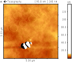
The helium beam of the ORION NanoFab was used to write circular structures with different doses into the body of a commercial silicon cantilever. The sample has been transferred to a Zeiss Merlin in which the AFM option is installed. The image in Fig. 1 shows an SEM image of the patterned area with the AFM tip in the vicinity. A great advantage of the combination of AFM and SEM is the ability to direct the AFM tip directly to the area of interest. In this case, the 5 µm x 5 µm sized helium beam patterned area.
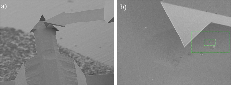
- Fig 1: a) SEM image of the patterned AFM cantilever (middle, tip pointing upwards) and AFM cantilever installed in AFM option
(upper right part of the image, tip pointing downwards). The patterned area is located in the middle of the image.
b) The SEM is used to guide the AFM tip towards the patterned area.
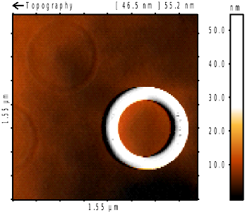
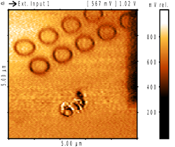
- Fig 2: AFM topography of the ORION NanoFab structured area. Structures generated with different dosage are visible. The circles on the left extrude over the surface plane where written with a dosage of 1 nC/µm2, the circles in the left part, protruding beneath the surface where generated by using an 0,08 nC/µm2.
The AFM topographical image from the center part of the patterned area is shown in Fig. 2. The circles in this area were written with a He dosage variation. The circles on the right protruding out from the surface were written with a dosage of 1 nC/µm2, the circles in the left part, visible as a small grove, where generated by using 0,08 nC/µm2.
Since the AFM generates 3 dimensional surface topographies, the images can also be plotted in 3D. The same area as displayed in Fig. 3 is shown in Fig 3 as a 3D surface plot. It can clearly be seen that the structures on the right side extrude some 10 nm out of the surface. The structures on the left, written with a 100 time lower dosage appear as shallow trenches in the surface.
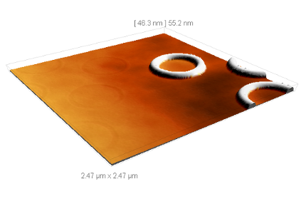
- Fig 3: AFM topograph of the ORION NanoFab structured area as 3D plot: A directional illumination has been added to the image to enhance small features like the patterns on the left side
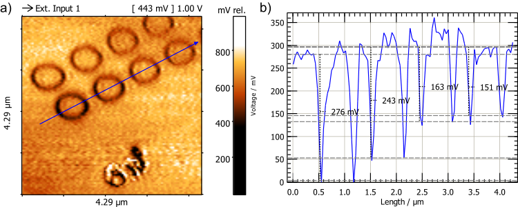
The AFM is not only able to plot the data in 3D but also provides the possibility to extract calibrated data from the images. In Fig. 4 the so called section tool was used to analyze the structures in width and height.
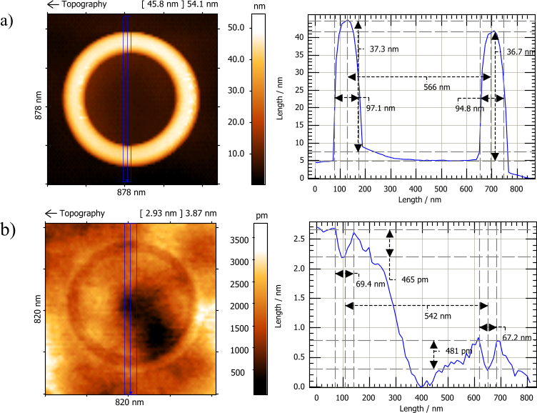
- Fig 4: Dimensional analysis of the generated nano patterns. a) Dimensional analysis of the structures written with 1 nC/µm2. The structure clearly protrudes from the surface plane. The height of the edge protruding the surface is around 40 nm. The width of the edge is around 100 nm. Additionally, it can be observed that the area inside the ring seems to be elevated in comparison to the surface area outside the ring structure. b) Dimensional analysis of the patterns generated with 0,08 nC/µm2. The structure observed here is a shallow trench with around 400 pm depth. The general surface flatness is larger than the step generated by removing material with the helium beam. The with of the trench is 60 nm, 30 nm less than the structures analyzed in a).
Since the He beam generated structures are only some hundred pico meter in z dimension, they are hardly visible in larger topographical AFM scans. The surface roughness is exceeding the structure height by a factor of 10 to 20 and obscure the structures. AFM phase imaging provides a great tool to enhance contrast in such situations. The ability of AFM phase imaging is illustrated in Fig 5, an area which has been structured by Helium milling with dosage gradient after extensive oxygen plasma cleaning of the sample and chamber. AFM topographical and phase data have been recorded simultaneously.
- Fig 5: Contrast enhancement by using AFM phase imaging.
a) A topographical image of the Si cantilever body. The circular pattern on the right side not clearly visible because the roughness of the surface is much larger than the z height of the generated pattern.
b) AFM phase image of the same area. The circular pattern is clearly visible. Topographical features only lead to minor contrast in phase images. The circular appears in slightly brighter color. This contrast is most probably generated by changed properties of the sample material.
Phase imaging generates a contrast based on variations in composition, adhesion, friction, viscoelasticity as well as other factors. Thereby, one is able to detect features which are not related to the surface topography. Since a prominent phase contrast can be seen here, it can be assumed that the investigated structure is not only a topographical feature. The interaction with the He beam must have had some influence to the sample material itself.
The AFM option provides the ability to analyze the chemical surface potential by Kelvin Force Probe Microscopy (KPFM). By this mode,
material contrast and potential differences in materials on the nm scale can be imaged. In case of surface structuring by a Gallium
FIB Saive et al. [1] have shown an effect on the potential distribution across the channel of a organic field effect transistor (OFET)
by using the Kelvin Probe Microscopy ability of an Auriga-installed AFM option.
In case of Helium milling, several publications report an effect of the dose selection on the milling results similar to what has been
shown above (see e.g. Boden et al. [2]). Suggestions regarding this effect is an implanting and possible bubbling of silicon by implanted
Helium ions. If this speculation is right, the implantation of the Helium Ions should have an effect on the chemical and other
characteristics of the material. The AFM option was used to investigate the nano patterns by KPFM to characterize possible changes in
material properties. The result is shown in Fig.6.
- Fig. 6: Topographical, Phase and KPFM image of the same sample area representing circular nanostructures.
a) The topographic contrast shows the pattern only with a very low contrast.
b) The phase image shows a diagonal line from the lower left corner to the upper third at the right side. One is also able to see the circles but with less contrast. In this part of the sample, an overview image was taken with the Orion, most probably leading to an He implantation or carbon deposition.
c) In the Kelvin probe image the circular pattern is clearly visible. A difference of around 200 mV can be measured. The diagonal line visible in the phase image can not be clearly observed.
Investigation of the He beam structured area shows a strong KPFM contrast of approximately 200 mV. This finding provides a strong argument that HE milling has influence on the electrical properties of Si respectively SiO. This assumption is also underlined by the fact that the change in the surface potential measured by KPFM seem to be dosage dependent. In Fig. 7, a profile through the lower line of circles on the KPFM image shows a reduction of the work function from left to right. This is in accordance to the dosage gradient used to generate the pattern.
- Fig. 7: Analysis of the work function in accordance to dose gradient. The dosage for writing each circle rises from right to left. The work function differences between the untreated surface areas and the circles also show a reduction from right to left. This implies a direct dependence between He dosage and work function difference.
By the results generated by the AFM it can be assumed that a high dose of Helium ions lead to an expansion of the Si respectively SiO
layer. A lower dose leads to a very low rate etching of the surface. Similar results are shown by Boden et al. [2].
A difference between treated and untreated surfaces can also be observed by material property sensitive AFM imaging techniques, Phase
and Kelvin probe imaging. Whereby areas treated with a very low dosage, resulting only from observation by HIM, seem to appear in the
phase images and areas treated with higher doses, milling with He, appear clearly in Kelvin probe images.
It can be speculated that the helium used for structuring may have been implanted in the Silicon and thereby generated this material
expansion and changed also electrical material properties. A direct dependence of the work function and used He dosage could be shown.
This information is very valuable in case of adjusting the right conditions for nano patterning. Additionally, information about material
property variation may lead to new lithography techniques.
No other method is able to provide this information as presented here about patterns at the low end of the nm scale. The combination
with the SEM in case of the Zeiss AFM option for Merlin FE SEM accelerated the work flow dramatically because the tip can be directed
to the area of interest under SEM guidance.
The presented measurements demonstrate the strength of the Carls Zeiss AFM option in analyzing very small patterns. The 3D topographical information on the nm and sub nm scale are able to give an extraordinary insight into details of nano patterned structures. Thereby giving scientists a tool in hand which enables to explain effects of the new technique of nano patterning by He and Ne with the ORION NanoFab and other nano structuring methods like FIB and electron beam lithography.
- Rebecca Saive, Lars Mueller, Eric Mankel, Wolfgang Kowalsky, Michael Kroeger,
Doping of TIPS-pentacene via Focused Ion Beam (FIB) exposure, Organic Electronics, Volume 14, Issue 6, June 2013, Pages 1570-1576 - S.A. Boden, Z. Moktadir, F.M. Alkhalil, H. Mizuta, H.N. Rutt, D.M. Bagnall,
Milling of extremely thin silicon-on-insulator using the helium ion microscope, EMC Abstract and Talk, EMC 2012