- DME Channel on YouTube
The characterisation of micro and nanostructured electrical devices is a mayor task in industry and research. Modern electronic components undergo a rapid mineaturisation process.
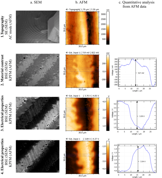
In this example, the potential distribution along the layer structure of an SMD capacitor is investigated.
An overview SE image is shown Fig. 1a. The applied voltage generates a topographical effect in the image.
BSE images with higher magnification (Fig. 2-4) show clearly the material-, and potential
difference. If the applied voltage is inversed, the BSE contrast also changes dramatically (Fig. 3-4).
The topographical and electrical properties can be examined in detail by AFM Kelvin Probe Force Microscopy (KPFM). By this method it is possible to characterize quantitatively the surface potential observed in the SEM images.
Without applying a voltage, KPFM shows a potential diffence of 527mV between the two electrode materials
(Fig 2).
A 4,5 V Battery has been used to apply a constant voltage to the capacitor. A potential diffrence of 4V
can be measured when the voltage is applied to the capacitor. If the voltage is inverted, a potential
diffenrence of -3.5V is measured wich equals the previously measured 4V minus the material specific 500 mV
(Fig. 3-4).